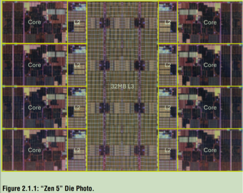
Codenamed “Zen 5,” AMD’s next-generation, energy-efficient high-performance x86 core targets a wide array of client, server, and embedded markets. Fabricated in TSMC’s 4nm FinFET process, the 55mm2 core complex (CCX), shown in Fig. 2.1.1., contains 8.6B transistors across eight cores, each with a 1MB private L2 cache and a shared 32MB L3 cache. The “Zen 5” implementation supports configurable FP256 and FP512 data paths. The “Zen 5” family includes a “Zen 5c” variant with increased density and power efficiency for key markets. The main design priorities for “Zen 5” are to improve per-core performance and energy efficiency, while aintaining similar area footprint as the prior generation [1]. The “Zen 5” core delivers a ~16% generational IPC increase in desktop PC applications [2] while supporting frequencies up to 5.7GHz [3].
Zen5是AMD的下一代高能效高性能 X86架构的cpu,面向广泛的客户端、服务器和嵌入式市场,采用TSMC的4nm finFET工艺,面积55mm2,86亿个晶体管,共有8个核,每个核包含1MB的L2缓存和32MB的L3缓存,还支持FP256和FP512数据通路。“Zen 5”的主要设计重点是提升单核性能和能效,同时保持与前代相近的面积在桌面PC应用中,“Zen 5”核心实现了约16%的IPC提升[2],同时支持最高5.7GHz的频率[3]
The “Zen 5” micro-architecture focuses on balanced throughput enhancements across the pipeline to achieve the performance uplift while maintaining power and area efficiency. Figure 2.1.2 presents key feature comparisons from the previous “Zen 4” generation. Improved branch prediction is combined with front-end parallelism, in the form of dual instruction fetch and micro-op cache pipes, to increase the dispatch width from six to eight micro-ops per cycle. To improve integer-based workloads, the ALU count increases to six units from the four found on all previous “Zen” generations.
Zen 5微架构聚焦于提升流水线各环节的均衡吞吐量,旨在实现性能跃升,同时降低功耗与面积。图2.1.2展示了其与前代“Zen 4”架构的关键特性对比。改进的分支预测技术与前端并行性设计(采用双指令取指与微操作缓存流水线)相结合,将每周期微操作(micro-op)发射宽度从6个提升至8个。为强化整数型工作负载处理能力,算术逻辑单元(ALU)数量从前代Zen架构的4个增至6个。(BTB branch target buffer缓存历史分支的目标地址)
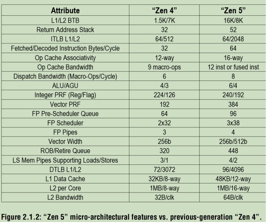
To make use of the additional execution hardware, a wider instruction window is implemented with a larger and higher throughput scheduler, register file, and retire queue. A fourth address generation unit is also inserted to support additional load and store pipes. The L1 data cache capacity is increased 50% to 48KB and 12 ways, while maintaining 4-cycle load-to-use performance. L2/L1 cache fill and victim bandwidth doubles to 64B per cycle. The design moved the majority of 8T SRAMs to 6T to increase density.
为了充分利用新增的执行硬件,设计中实现了更宽的指令窗口,并配备了更大规模、更高吞吐量的调度器、寄存器堆及退役队列(将完成的指令压入这个队列)。此外,设计中还增设了第四个地址生成单元,以支持额外的加载与存储流水线。一级数据缓存容量提升50%至48KB,采用12路组相联结构,同时保持4周期的加载至使用延迟性能。二级缓存与一级缓存间的填充及失效带宽翻倍,达到每周期64字节。设计中将大部分8晶体管SRAM替换为6晶体管结构,以提升存储密度。
The “Zen 5” floating point (FP) data path increases to 512b from 256b on “Zen 4,” doubling the bandwidth for advanced vector extension (AVX512) instructions. Other notable FP changes include a doubling of dedicated FP registers, enhanced out-of-order scheduling capability, a reduction of the minimum FPADD latency to 2-cycles, and a doubling of the bandwidth for INT8, INT16, and BFLOAT16 AI formats. Through the use of improved on-die sensors, AC capacitance () monitors, and di/dt-based adaptive clocking, “Zen 5” can achieve full AVX512 performance at the peak core frequency. The FP implementation allows for the upper 256b data path to be power gated at boot time. This reverts the FP to the double-pumped AVX512 implementation used on “Zen 4,” achieving similar power efficiency by also using an independent mesh clock to gate the upper 256b data path [4]. This configurable implementation also makes it simple to create discrete 256b data path FP variants for product flexibility.
“Zen 5”的浮点(FP)数据路径位宽从“Zen 4”的256位提升至512位,使高级向量扩展(AVX512)指令的带宽翻倍。其他值得关注的浮点改进包括:专用浮点寄存器数量翻倍、增强的乱序调度能力、浮点加法(FPADD)最小延迟降至2个周期,以及INT8、INT16和BFLOAT16人工智能格式的数据带宽翻倍。通过改进的片上传感器、交流电容()(由于信号快速变化在导线附近产生的电容)监测和基于电流变化率(di/dt)的自适应时钟技术,“Zen 5”可在峰值核心频率下实现完整的AVX512性能。其浮点实现方案允许在启动时对上层256位数据路径进行电源门控,这使得浮点单元回归到“Zen 4”所采用的双泵浦AVX512实现方式——通过独立的网状时钟对上层256位数据路径进行门控,在实现相近能效的同时[4]。这种可配置的实现方式还简化了独立256位数据路径浮点变体的创建,为产品灵活设计提供了便利。
“Zen 5” fits 30% more transistors into the same CCX area as “Zen 4” via numerous advancements across core implementation, 4nm process technology, and cache design. The bulk of the area improvements are in cache design and stacking technology. “Zen 4” significantly improved the stacking area efficiency relative to “Zen 3”, and “Zen 5” continues this trend with a solution that requires minimal core complex die (CCD) area.
通过4nm制程工艺及缓存设计等多方面的改进,在相同CCX面积的情况下“Zen 5”比“Zen 4”多容纳了30%的晶体管。面积使用效率的提升主要来自缓存设计与堆叠技术的优化。“Zen 4”相对于“Zen 3”已显著提升了堆叠面积效率,而“Zen 5”延续了这一趋势,采用了缩小极小核心复合体芯片(CCD)面积的解决方案。
“Zen 5” L2 is a fast, private cache with 1MB per core as in “Zen 4,” however, the bandwidth between the core and L2 is doubled from 32B/cycle to 64B/cycle. Additionally, the L2 associativity doubles from 8-ways to 16-ways. Logic device area is reducing faster than 6T SRAM in modern process technologies, so cache floorplans must be increasingly flexible to maintain density. Despite the increased performance of the “Zen 5” L2, the density is improved by 11% (process technology neutral) relative to “Zen 4” via flfloorplan changes shown in Fig. 2.1.3.
"Zen 5"架构的二级缓存(L2)如同"Zen 4"一样,每个核心独占1MB高速私有缓存;不过,其核心与L2 cache之间的带宽提升了一倍,从每周期32字节增加至每周期64字节。此外,L2的关联性也翻倍,从8路提升至16路。在现代制程技术中,逻辑器件的面积缩减速度快于6T SRAM,因此,为维持存储密度,缓存布局必须变得更加灵活。尽管“Zen 5”的二级缓存(L2)性能有所提升,但通过图2.1.3所示的布局调整,其密度相比“Zen 4”改进了11%。(与工艺制程没有关系)
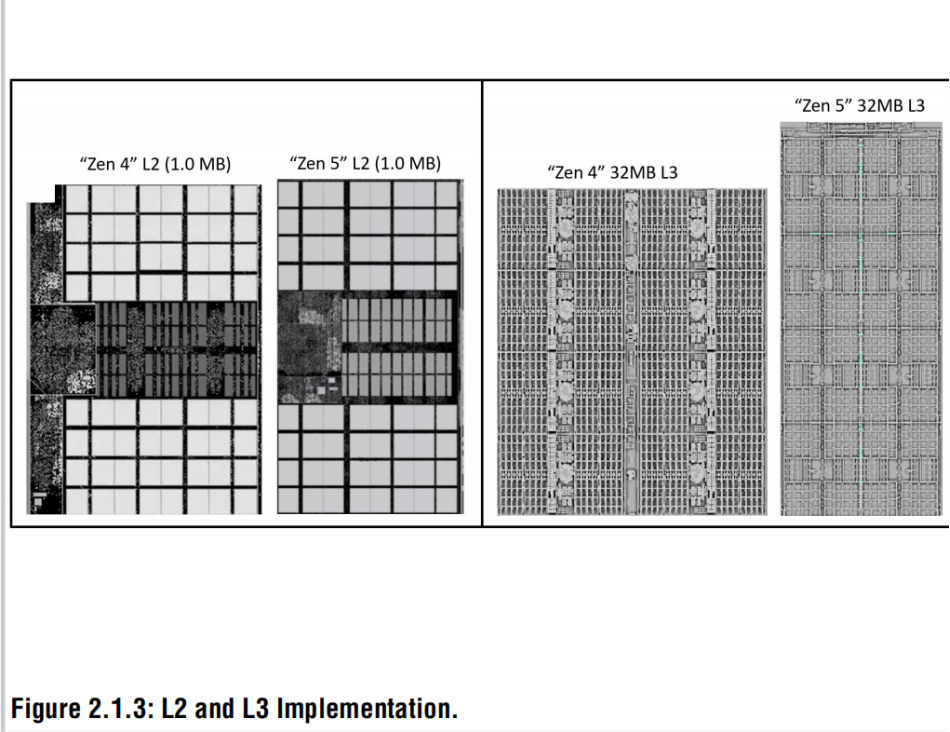
The “Zen 3” and “Zen 4” L3 “ring” fabric topology [5] is replaced by a mesh topology which reduces latency and increases bandwidth, especially for configurations with higher core counts. New L3 macros are created to achieve higher density. L3 data macro capacity is doubled, and its density improved by 10%. Circuit techniques are used to mitigate the frequency loss that typically occurs from doubling the capacity of SRAM macros. The capacity of each tag macro is doubled which leads to an 11% improvement in density.
“Zen 3”与“Zen 4”采用的L3环形拓扑[5] 被替换为网状拓扑,此举有效降低延迟并提升带宽,在高核心数配置中尤为显著。为实现更高密度,全新设计了L3宏单元:L3数据宏单元容量翻倍,密度提升10%;通过电路设计技术缓解了SRAM宏单元容量翻倍时常见的频率损失问题;标签宏单元容量同步翻倍,密度随之提高11%。
Another primary “Zen 5” objective is to drive an energy-efficient, high-IPC machine that scales across a variety of workloads. Driving high IPC and new features, such as FP512, typically comes with more transistors and is challenging for frequency/power attainment.
“Zen 5”的另一核心设计目标是打造高能效、高IPC(instructions per cycle)的架构,并确保可以扩展到不同的应用中。然而,驱动高IPC及新增特性如FP512,需要集成更多晶体管,这使得频率提升与功耗控制难以兼顾。
Unlocking improvements in transistor density to reduce switching and leakage power are key for delivering an efficient, high-IPC, 5.7GHz design. In addition to density improvements enabled by the geometric process shrink from a 5nm process to a 4nm process, PD methodology innovations such as array efficiency, SRAM optimizations, standard cell optimizations, design technology co-optimization, and utilization improvements results in higher transistor density.
要实现5.7GHz高频、高IPC且能效优异的设计,关键在于提升晶体管密度以降低开关功耗与漏电功耗。除借助芯片工艺,从5nm升级至4nm,实现的晶体管密度增长外,物理设计方法论创新——包括存储党员阵列效率比(阵列面积与缓存总面积之比)提升、SRAM优化、标准单元优化、设计工艺协同优化以及利用率改进——也共同推动了晶体管密度的进一步跃升。
Significant emphasis is placed on switching power, C_AC, and leakage with detailed tracking of power for each RTL feature. Use of numerous RTL and PD power reduction methods enables “Zen 5” to reduce /IPC cost.
"Zen 5"设计中重点优化了开关功耗及漏电功耗,并追踪每个RTL模块的详细功耗,通过应用大量RTL与PD的功耗优化技术(S家的VCLP工具),成功降低了(/IPC)。
The physical design focuses on timing and power co-optimization in the synthesis, place, and route (SAPR) tools to reduce dynamic and leakage power. The “Zen 5” breakdown is shown in Fig. 2.1.4. Macro power contribution is higher relative to “Zen 4” due to the larger array structures which enable higher performance.
在物理设计中,针对时序,可以通过综合、布局布线(SAPR)工具进行优化,以降低动态功耗与漏电功耗。"Zen 5"的功耗构成分析见图2.1.4。由于采用更大规模的阵列结构以实现更高性能,其宏单元(已经设计好的功能块,比如一个模拟模块,直接插到后端中)功耗占比相较"Zen 4"有所提升。
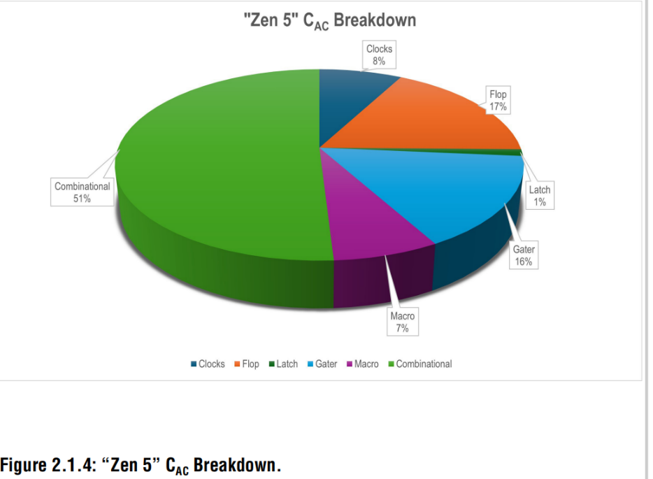
Contributions from flop/gater/clock are lower. High emphasis is put on multi-bit flop banking optimizations as well as attention to the flop cell palette and design usage. Clock gater is optimized with improved clock-gating cells and clock-tree synthesis (CTS) methodology. swap algorithms incorporated optimizations to better balance leakage, power, and frequency attainment.
触发器/门电路/时钟网络的功耗占比有所降低。设计重点集中于:多比特触发器组优化触发器单元库的精选与使用策略优化时钟门控(clock gater)通过以下手段升级:改进型时钟门控单元创新的时钟树综合方法学交换算法引入优化机制,更精准平衡漏电功耗、动态功耗与频率目标。
As with past “Zen” products [1], AMD utilizes the AM5 package for “Zen 5” desktop comprised of the CCX, a system management unit (SMU), test/debug logic, and dual Infinity Fabric™ On-Package (IFOP) SerDes links. One or two CCDs are once again combined with a 6nm IO die (IOD) to deliver a broad range of “Zen 5”-based client desktop products codenamed “Granite Ridge” ranging from 6-core to 16-core.
如同历代“Zen”产品[1],AMD在“Zen 5”桌面处理器中继续采用AM5封装,其包含:CCX、一个系统管理单元(SMU)、测试/调试逻辑、用两个IF互联、SerDes链路。1个或2个CCD与6nm I/O芯片连接,提供代号“Granite Ridge”的“Zen 5”客户端桌面产品系列,核心数覆盖6核至16核。
An over-arching goal for “Zen 5” is to create a family strategy to extend the dynamic range and leverage the “Zen 5” core in a wider set of use-cases [3]. Setting this strategy early-on allows the team to push the “Zen 5” core into the client notebook product offering as well as desktop. Using versions of the “Zen 5” core with a 256b flfloating point data path width, multiple CCX variants are developed for the “Strix” product family including a 4 “Zen 5” core plus 16MB L3 variant and an 8 “Zen 5c” plus 8MB L3 variant [6] as shown in Fig. 2.1.5. These “Zen 5” family options are instrumental in allowing AMD to deliver “Zen 5” core performance into laptop products with initial product offerings available at the same time as our desktop platforms, thus delivering optimal performance, power, and cost targets for multiple market segments.
"Zen 5"的核心战略目标是构建统一的架构家族策略,以扩展动态性能范围并将"Zen 5"应用于更广泛的使用场景[3]。该策略的早期制定使团队能将"Zen 5"核心同时推向笔记本和PC。通过采用256位浮点数据路径的"Zen 5"核心变体,为"Strix"产品家族开发了多款CCX配置:4个"Zen 5"核心 + 16MB三级缓存8个"Zen 5c"核心 + 8MB三级缓存[6](架构拓扑见图2.1.5)这些方案使AMD得以"Zen 5"加入笔记本产品,实现与桌面平台同步上市,从而在多细分市场上达成性能、功耗与成本的最优平衡。
“Zen 5” performance per watt is improved versus “Zen 4” by delivering more performance at fixed power. The “Zen 5” architecture is wider resulting in more IPC and total . Figure 2.1.6 [7] shows that 1T Cinebench R23 (CBR23) performance per watt improved at high and medium power envelopes. As power is reduced, the performance of the current and previous generations approach a cross-over point at lower power envelopes.
相较于“Zen 4”,“Zen 5”的能效比(性能/瓦特)通过同功耗下提供更高性能实现显著提升。更宽的“Zen 5”架构(增加执行单元/指令发射宽度)带来更高IPC与。图2.1.6 [7]显示:高/中功耗区间:单线程Cinebench R23(CBR23)能效比显著优化低功耗区间:两代架构性能趋近,于特定功耗阈值出现交汇点
在这里插入图片描述
Client programs leverage “Zen 5c” cores which have lower , area, and frequency to deliver better energy-efficiency at the lower power envelopes and maximize nT performance. Figure 2.1.7 [8,9] shows the performance uplift of the 12-core 9900X vs. the 24-core 14900K and the 8-core 9700X vs. the 20-core 14700K across a variety of workloads. The uplift varies from 1% for office productivity and up to 40% for Handbrake, which makes use of AVX512 instructions.
客户端程序借助“Zen 5c”核心,其功耗、面积及频率更低,在更低功耗范围内实现了更优的能效表现,并最大化了nT性能(注:nT通常指每瓦特性能或特定场景下的综合性能指标)。如图2.1.7 [8,9]所示,在各类工作负载下,12核9900X处理器的性能相较于24核14900K,以及8核9700X相较于20核14700K均有提升。具体来看,办公生产力任务的性能提升幅度仅为1%,而依赖AVX512指令的视频转换软件Handbrake的性能提升幅度则高达40%。
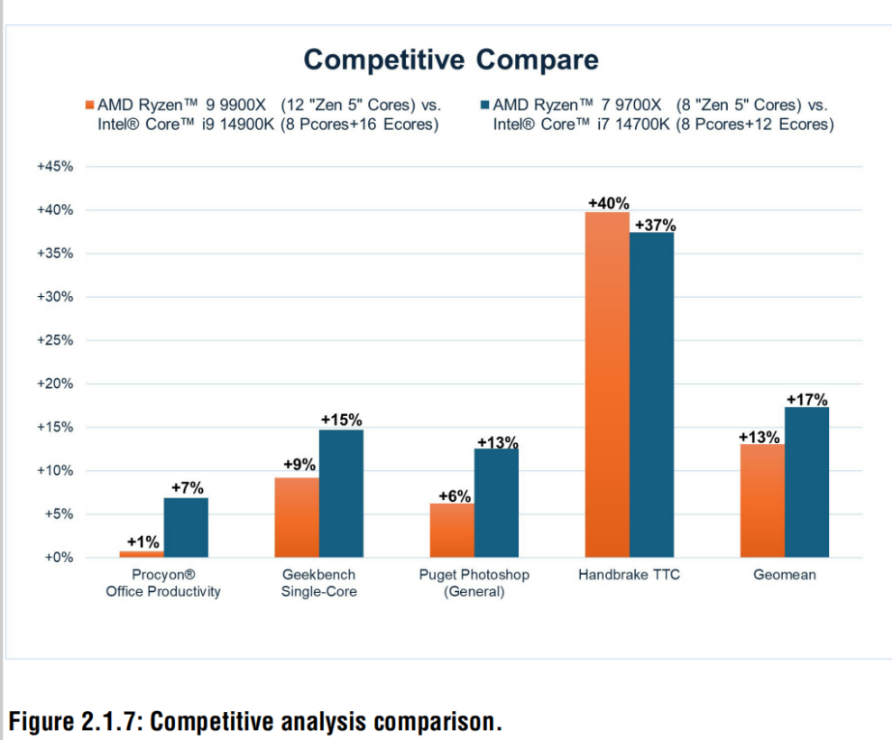
Despite having half or even less of the total core count, the 9900X and 9700X have a 13% and 17% geomean uplift over the 14900K and 14700K, respectively. Usage of high-efficiency cores and aggressive power-saving physical design techniques enables a 17% improvement in CBR23 nT IPC.
尽管核心总数仅为竞品一半甚至更少,但Ryzen 9900X与9700X仍分别实现了:13%和17%几何平均性能提升(前后两个处理器性能之比)(对比Core i9-14900K和14700K) ,高效能核心的设计与先进的低功耗物理设计相结合,使Cinebench R23多线程测试中的IPC提升达17%。
References:
[1] B. Munger et al., “Zen 4: The AMD 5nm 5.7GHz x86-64 Microprocessor Core,” ISSCC, pp. 38-39, 2023.
[2] GNR-03: Testing as of May 2024 by AMD Performance labs. “Zen 5” system configured with: Ryzen 9 9950X GIGABYTE X670E AORUS MASTER motherboard, Balanced, DDR5-6000, Radeon RX 7900 XTX, VBS=ON, SAM=ON, KRACKENX63 vs. “Zen 4” system configured with: Ryzen 7 7700X, ASUS ROG Crosshair X670E motherboard, Balanced, DDR5-6000, Radeon RX 7900 XTX, VBS=ON, SAM=ON, KRAKENX62 {FixedFrequency=4.0 GHz}. Applications tested include: Handbrake, League of Legends, FarCry 6, Puget Adobe
Premiere Pro, 3DMark Physics, Kraken, Blender, Cinebench (n-thread), Geekbench, Octane, Speedometer, and WebXPRT. System manufacturers may vary configurations, yielding different results. GNR-03.
[3] B. Cohen, M. Subramony, M. Clark, “Next Generation “Zen 5” Core,” Hot Chips, 2024.
[4] T. Singh et al., “Zen 2: The AMD 7nm Energy-Efficient High-Performance x86-64 Microprocessor Core,” ISSCC, pp. 42-43, 2020.
[5] T. Burd, et al., “Zen 3: The AMD 2nd-Generation 7nm x86-64 Microprocessor Core,” ISSCC, pp. 54-55, 2022.
[6] T. Burd et al., “Zen 4c: The AMD 5nm Area-Optimized x86-64 Microprocessor Core,” ISSCC, pp. 38-40, 2024.
[7] GNR-19: Testing as of Sept. 2024 by AMD Performance Labs on test systems configured as follows: AMD Ryzen 9 7950X, Ryzen 9 9950X, AMD “Splinter” reference motherboard. 2x8GB dual channel DDR5-5600; Samsung 970 Pro SSD; Radeon RX 6800S graphics (461.4 driver), VBS & SAM off, Windows 10 professional (x64) 20H2 on the following application: Cinebench R23 1T. Results may vary and are based on several factors, including system configuration, application, and software. GNR-19.
[8] GNR-06: Testing as of June 2024 by AMD Performance Labs on test systems configured as follows: AMD Ryzen 9 9900X CPU system: GIGABYTE X670E AORUS MASTER, Balanced, DDR5-6000, Radeon RX 7900 XTX GPU, VBS=On,SAM=On, KRACKENX63 vs. similarly configured Intel Core i9-14900K system: MSI MEG Z790 ACE MAX (MS-7D86), Balanced, DDR5-6000, Radeon RX 7900 XTX, VBS=On, SAM=On, KRAKENX63, {Profile=Intel Default} on the following applications/games: Procyon Office, Geekbench 6.2.1 Single Core, Puget Photoshop (general), Blender (classroom TTC), Handbrake TTC, Borderlands3, DOTA2, Hitman3, Cyberpunk2077, F12023, and Horizon Zero Dawn. All games tested at 1080p resolution. System manufacturers may vary configurations, yielding different results. GNR-06.
[9] GNR-07: Testing as of June 2024 by AMD Performance Labs on test systems configured as follows: AMD Ryzen 7 9700X CPU system: GIGABYTE X670E AORUS MASTER, Balanced, DDR5-6000, Radeon RX 7900 XTX, VBS=On,SAM=On, KRACKENX63 vs. similarly configured Intel Core i7-14700K system: MSI MEG Z790 ACE MAX (MS-7D86), Balanced, DDR5-6000, Radeon RX 7900 XTX, VBS=On, SAM=On, KRAKENX63, {Profile=Intel Default} on the following applications/games: 7-Zip, Procyon Office Productivity, GeekBench 5.4.6 Single Core, Puget Adobe Photoshop, Handbrake, Borderlands 3, DOTA2, Hitman3, Cyberpunk2077, F12023, and Horizon Zero Dawn. All games tested at 1080p resolution. System manufacturers may vary configurations, yielding different results. GNR-07


ES模块(ESM)、与传统Webpack对比、Rollup打包)


-- 基础概念)
![week1-[分支结构]中位数](http://pic.xiahunao.cn/week1-[分支结构]中位数)
![[激光原理与应用-259]:理论 - 几何光学 - 平面镜的反射、平面透镜的折射、平面镜的反射成像、平面透镜的成像的规律](http://pic.xiahunao.cn/[激光原理与应用-259]:理论 - 几何光学 - 平面镜的反射、平面透镜的折射、平面镜的反射成像、平面透镜的成像的规律)
